| |
|
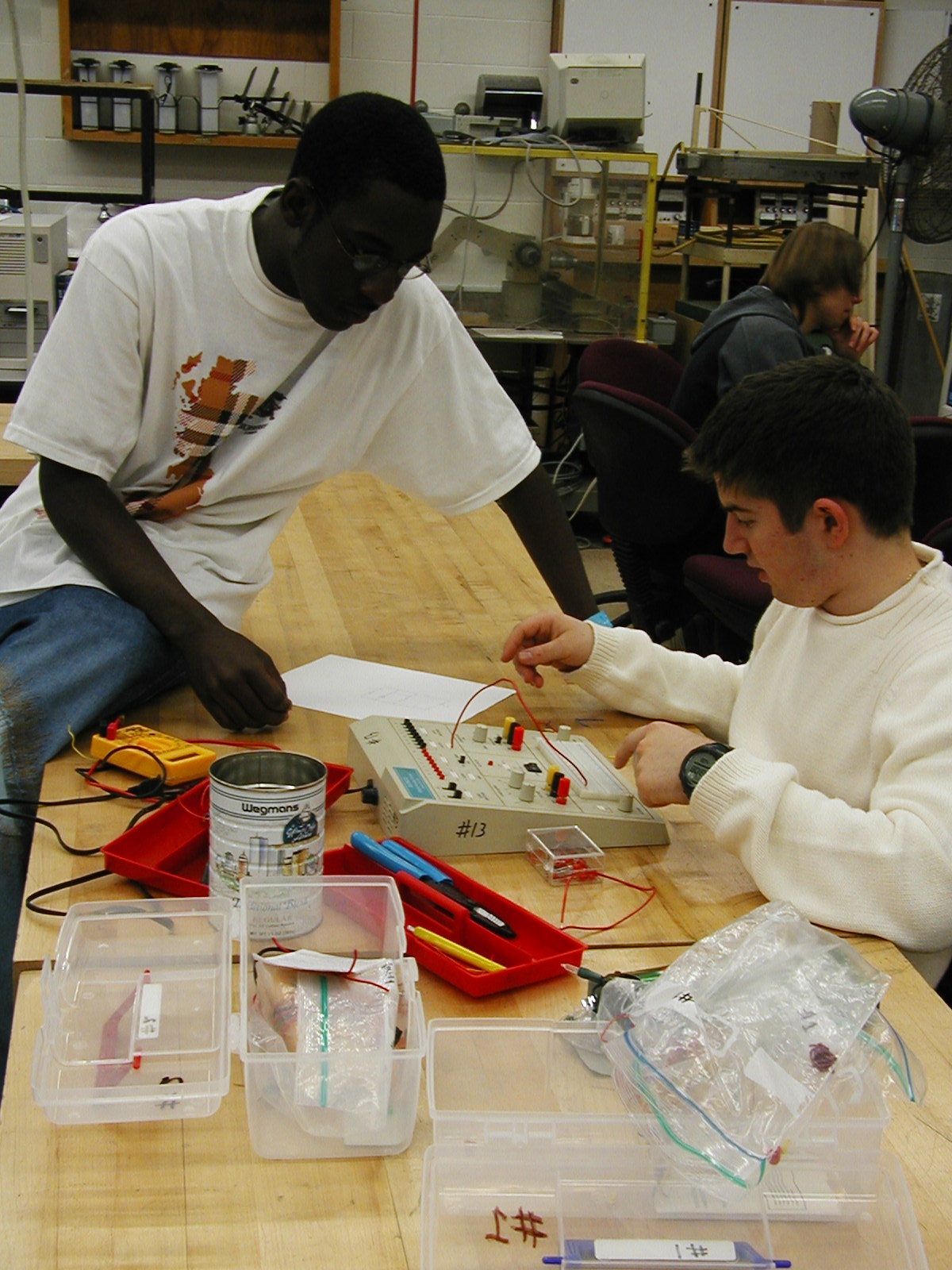
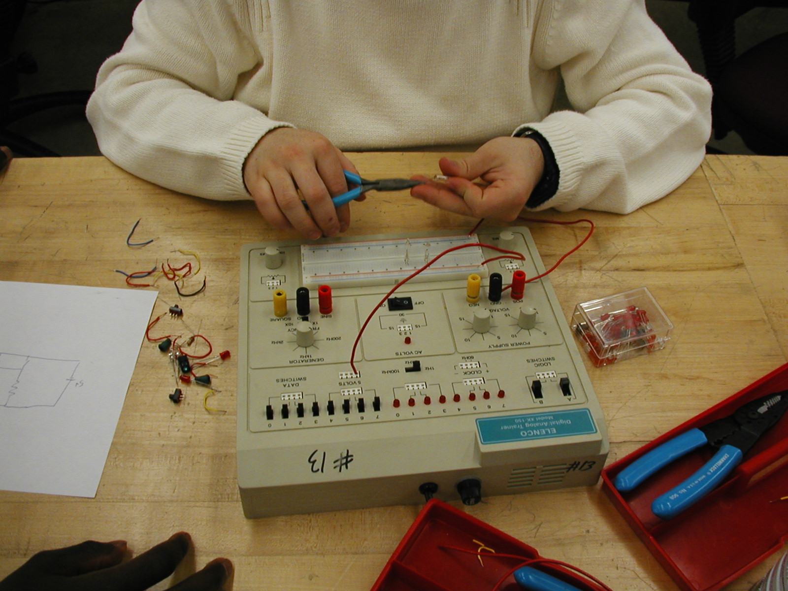
| 1) Kobina and Brandon work out the details. |
Enter content here
|
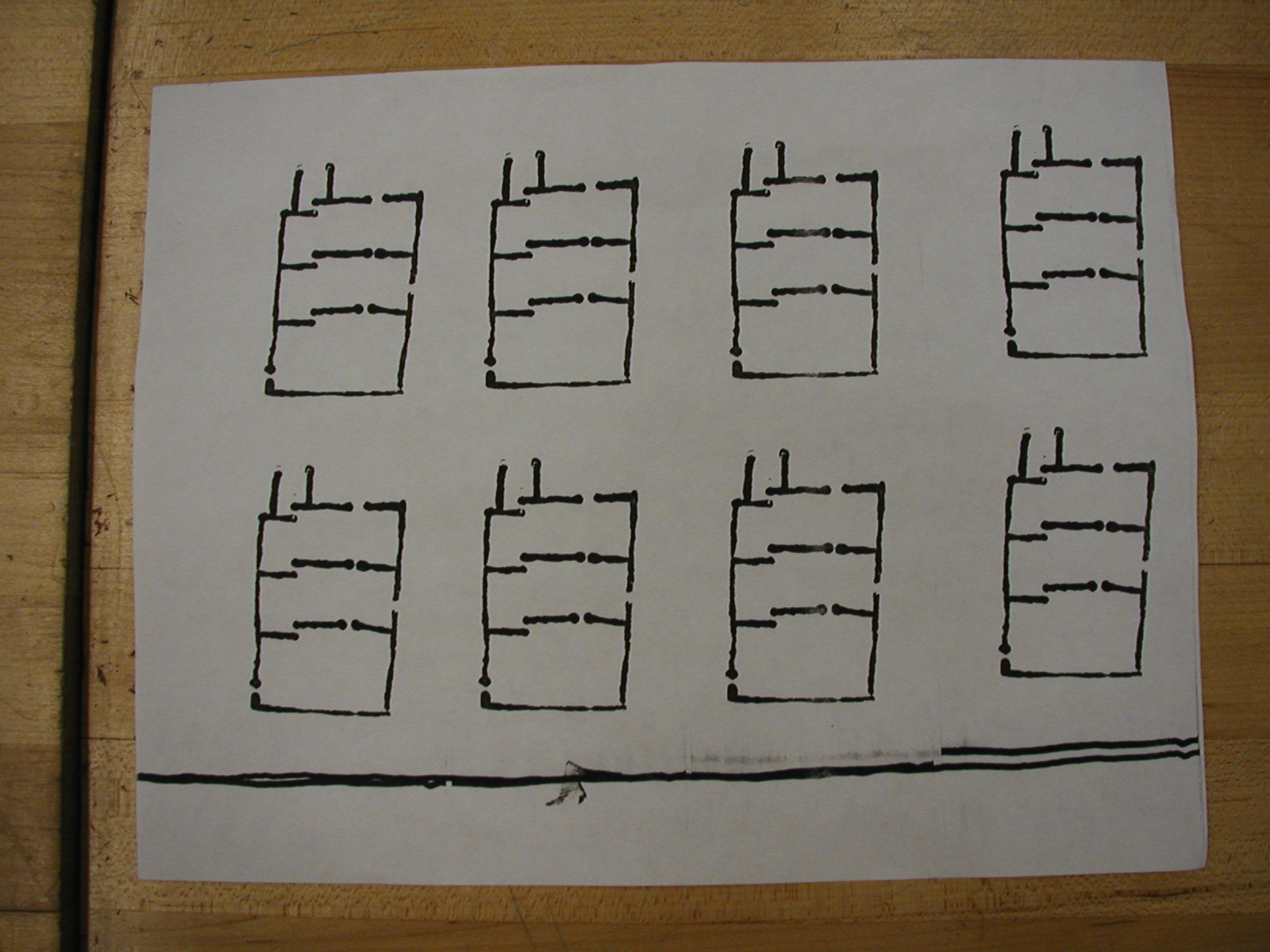
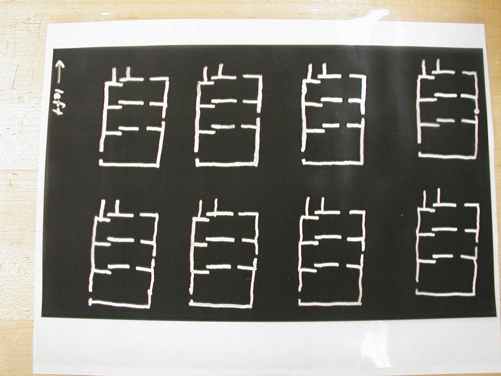
| 4) The original artwork for the circuit board. |
|
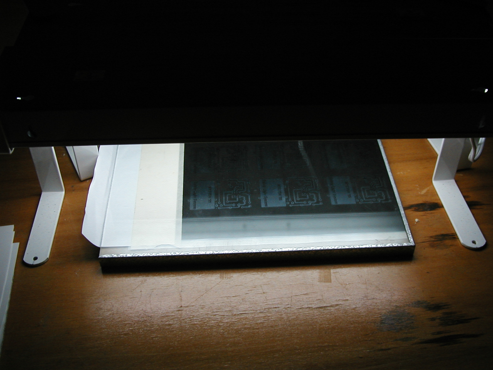
| 7) Exposing the photosensitised copper clad board to UV light. |
|
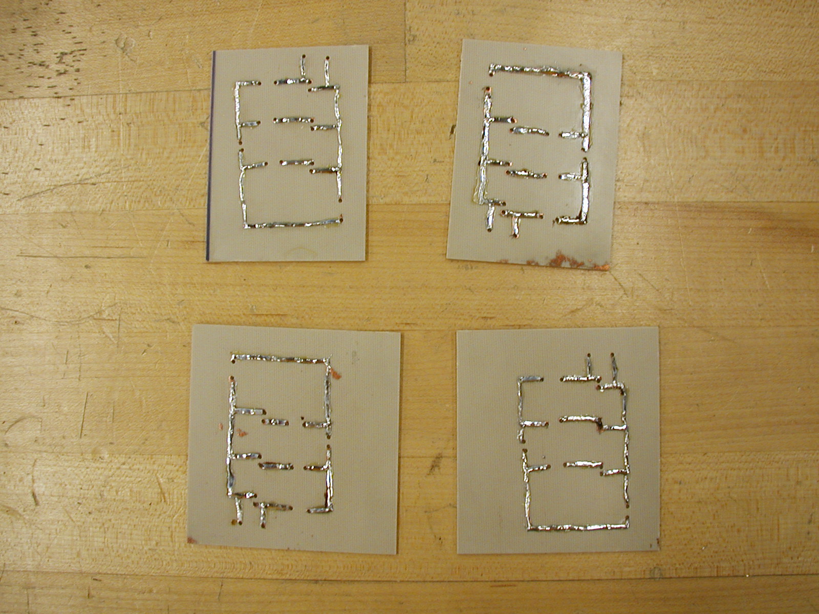
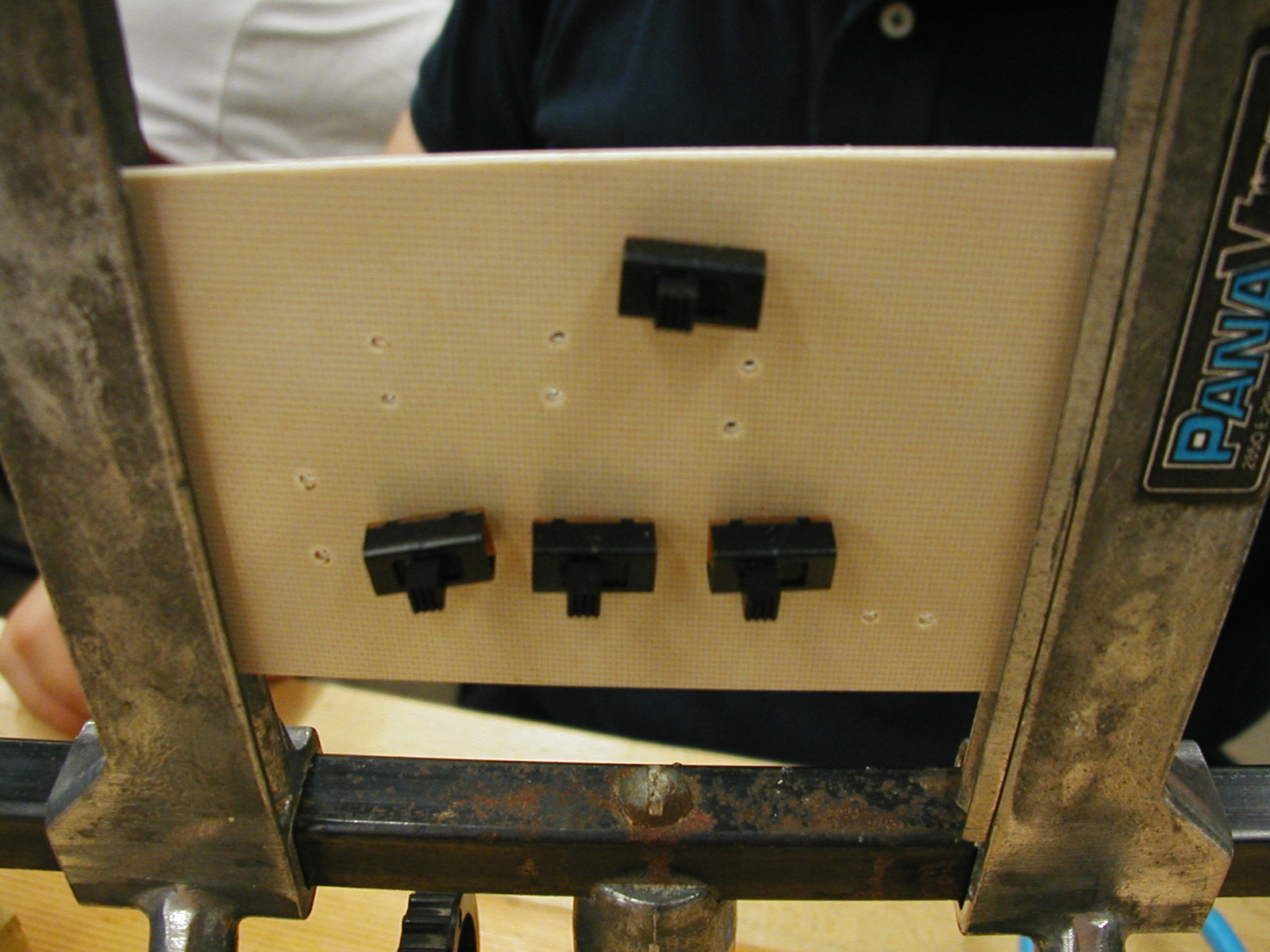
| 10) Four tinned printed circuit boards. |
|
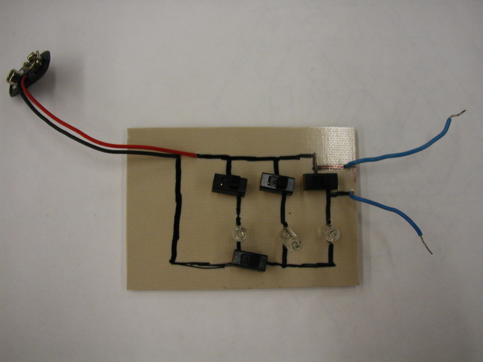
| 13) Almost complete! |
|
| |
|
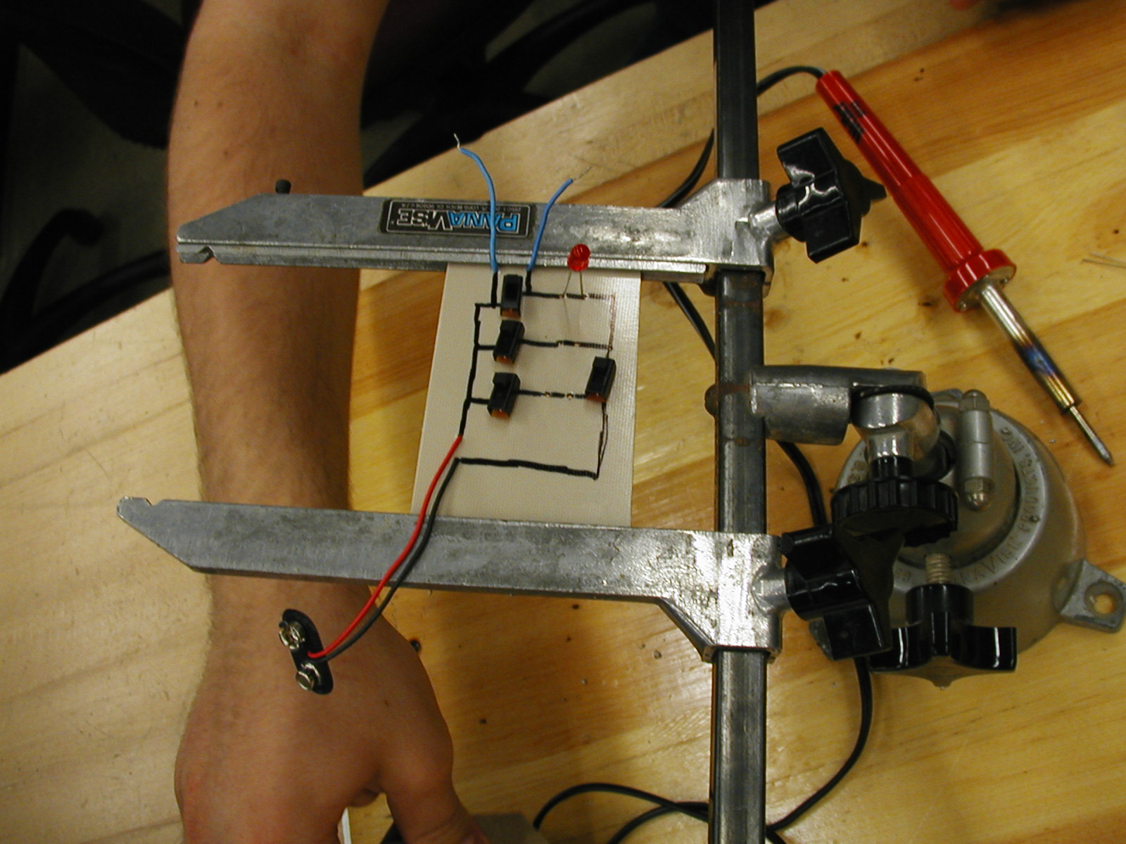
| 2) Building the prototype. |
Enter content here
|
| 5) The reverse image is ready to be transfered to the copper clad board. |
|
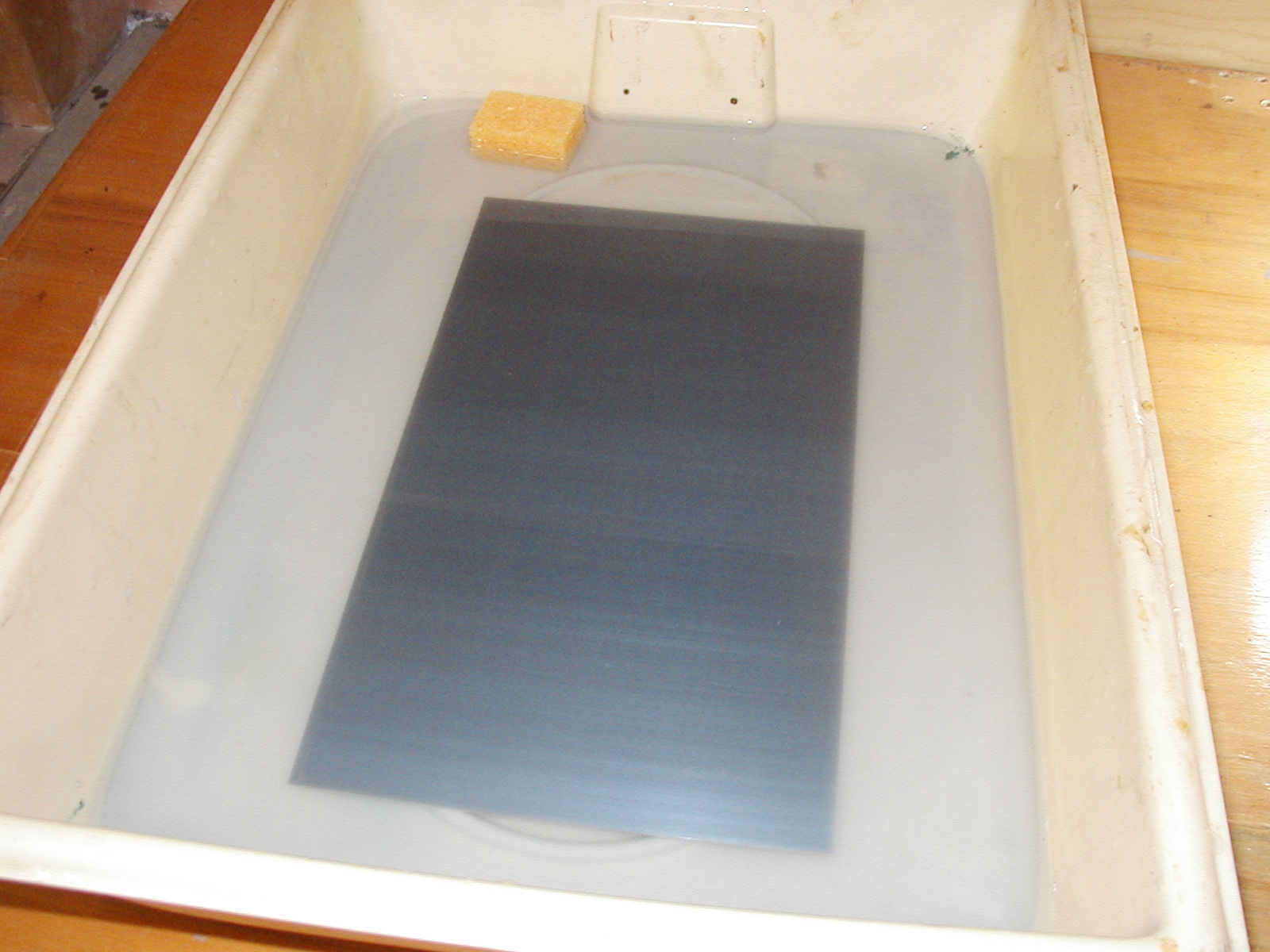
| 8) Developing the exposed copper clad board. |
|
| 11) Adding the components. |
|
| 14) The finished PCB is ready for the physics lab. |
|
| |
|
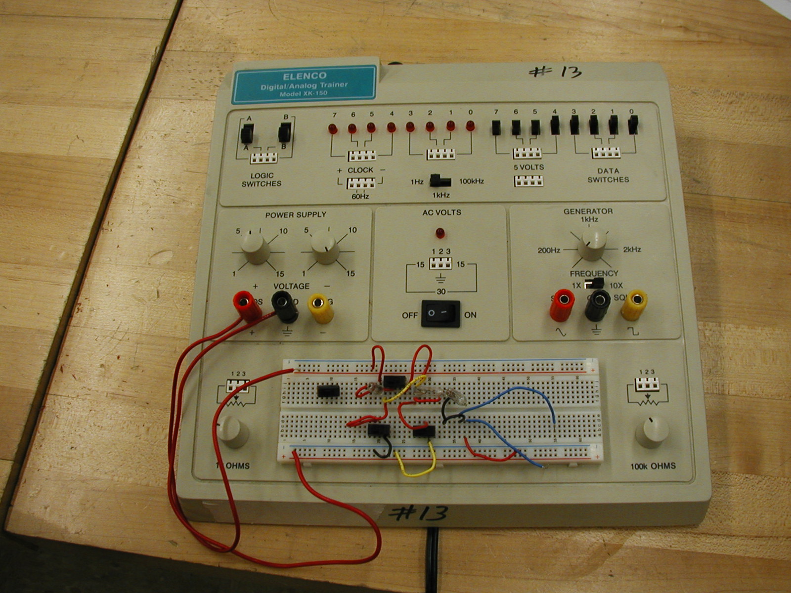
| 3) The prototype is complete and working. |
Enter content here
|
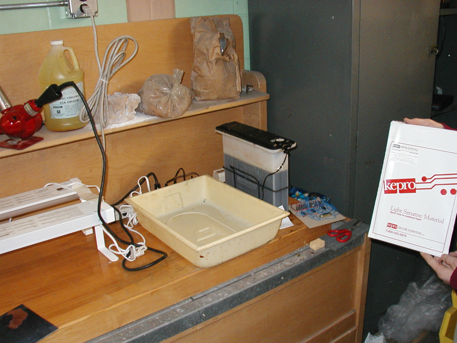
| 6) The ultraviolet exposure light, developing tray, and etching tank for producing the PCB. |
|
| 9) After etching and drilling, the copper path of the board is tinned. |
|
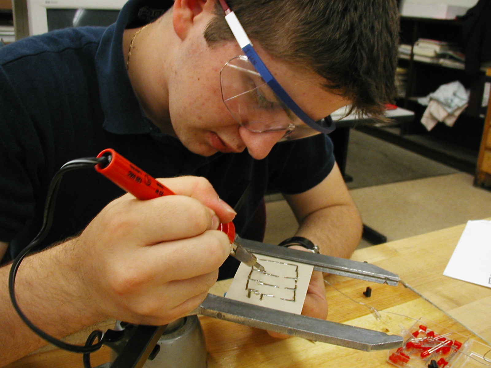
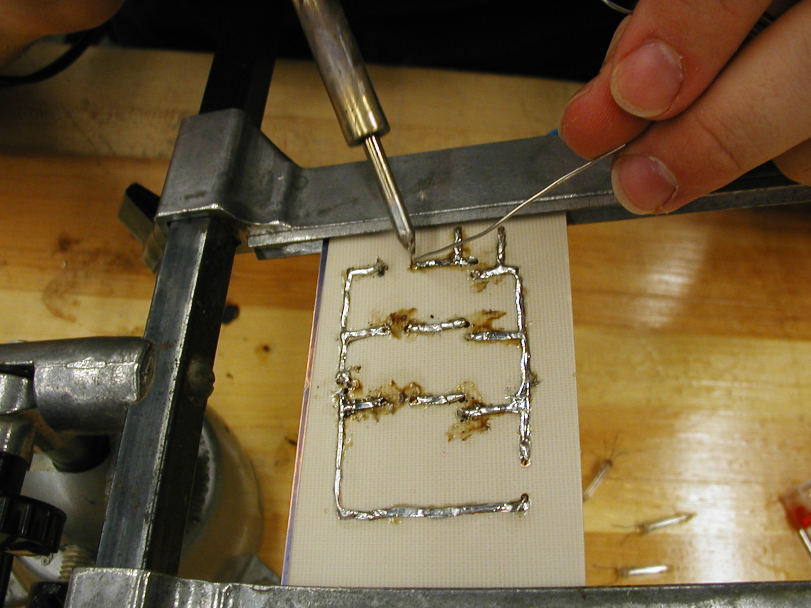
| 12) Soldering the components onto the PCB. |
|
|
 |
|
|
| |